Components of an on-premises semiconductor design environment
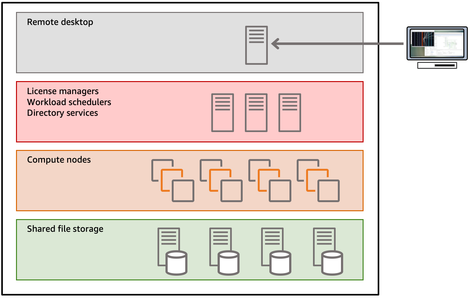
The following figure shows a simple view of a typical on-premises semiconductor and electronics design environment. This diagram has the necessary components to run the entire workflow. As you continue through this guide, make sure to reference this diagram as a comparison to the infrastructure that is launched on AWS. That is, all of the components in this diagram are launched and further optimized on AWS.
Traditional on-premises environment
