This whitepaper is for historical reference only. Some content might be outdated and some links might not be available.
Enable secure collaboration chambers with third parties
Across the entire semiconductor industry, the need for collaboration is part of the design process, fabrication, and product manufacturing. AWS allows you to securely collaborate with third-party IP providers, EDA tool vendors, foundries, and contract manufacturers. For example, you might have a requirement to work with a third-party IP provider or contract engineering team to create or validate a portion of your system-on-chip (SoC). Using AWS for collaboration makes it possible to segregate roles and data, lock down the environment to only authorized users, and monitor activity in the environment.
When trying to create similar collaborative environments in your on-premises data center,
you might have the ability to isolate users and groups through existing network policies;
however, you are still allowing external access to your internal infrastructure, and the
collaboration environment is not scalable. On AWS, you can set up completely separate, secure,
and scalable environments that allow you to isolate access to just what is needed for the
collaborative effort. This approach can be accomplished in several ways on AWS, but typically
starts with a separate Amazon Virtual Private Cloud (Amazon VPC)
This section includes three collaboration examples specific to the semiconductor industry:
Each of these examples leverages a separate VPC to ensure a secure, isolated chamber that enables fine-grained control that restricts the environment to only the data and applications necessary for that specific project.
Collaboration with IP providers and EDA tool vendors (ISVs)
From customer specifications to silicon, tool vendors and IP providers are a critical part of the entire workflow. Acquiring the latest version of tools and libraries is a manual process, that remains largely unmonitored and untracked.
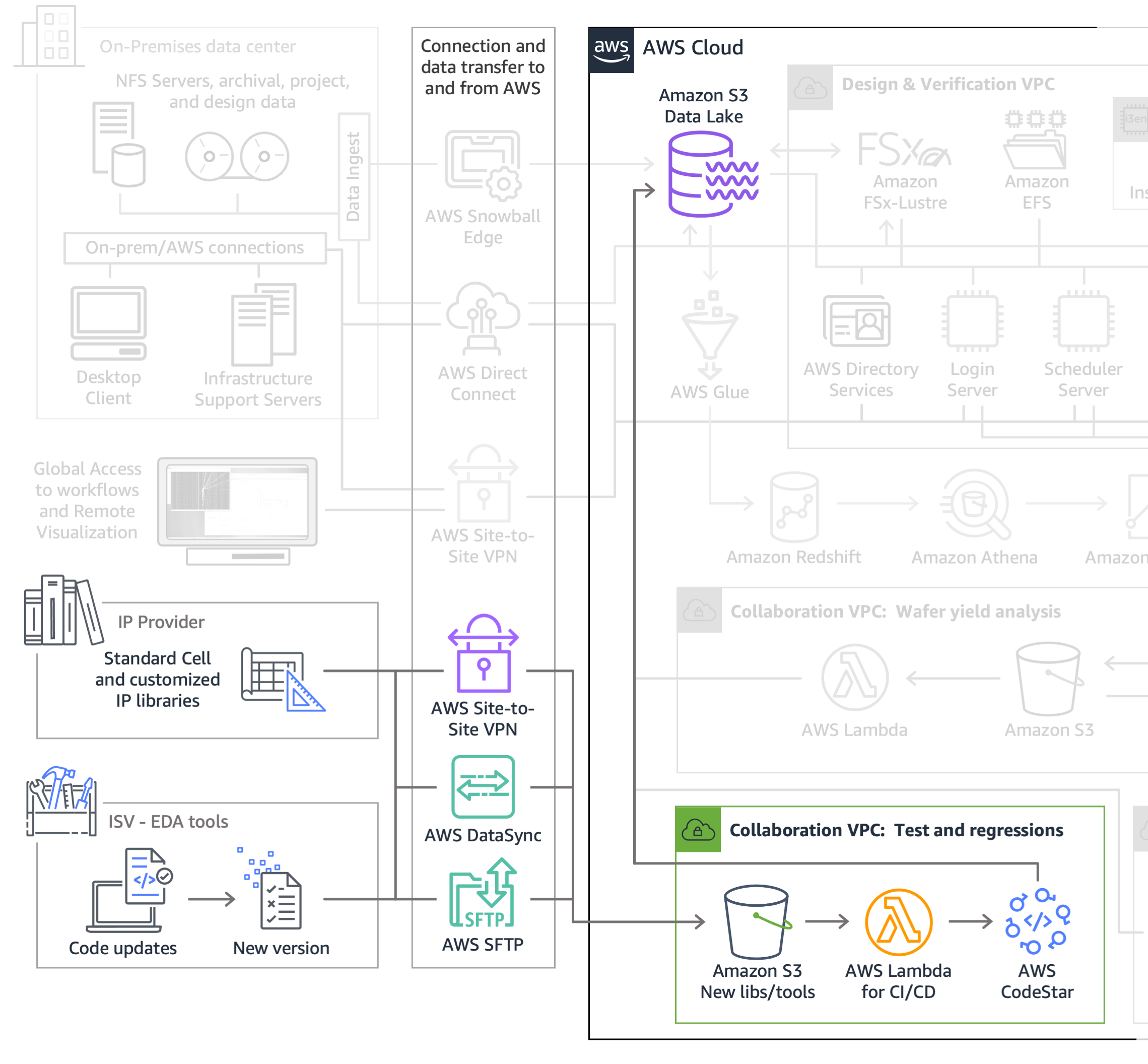
The following figure shows a collaboration VPC for test and regressions.
Collaboration with IP providers and EDA tool vendors (ISVs)
In this figure, the collaboration VPC is set up to allow for inbound transfers from
both the tool and IP providers. You can allow inbound transfers using any of the AWS Transfer Family
Collaboration with foundry
After sending your GDSII file to the foundry, the wafer fabrication process has traditionally been obfuscated from the chip design teams. Launching a separate VPC to enable collaboration with just your foundry can result in robust analytics, a reduction in time-to-market, and increased ROI. The following figure shows the wafer yield analysis from collaboration with your foundry.
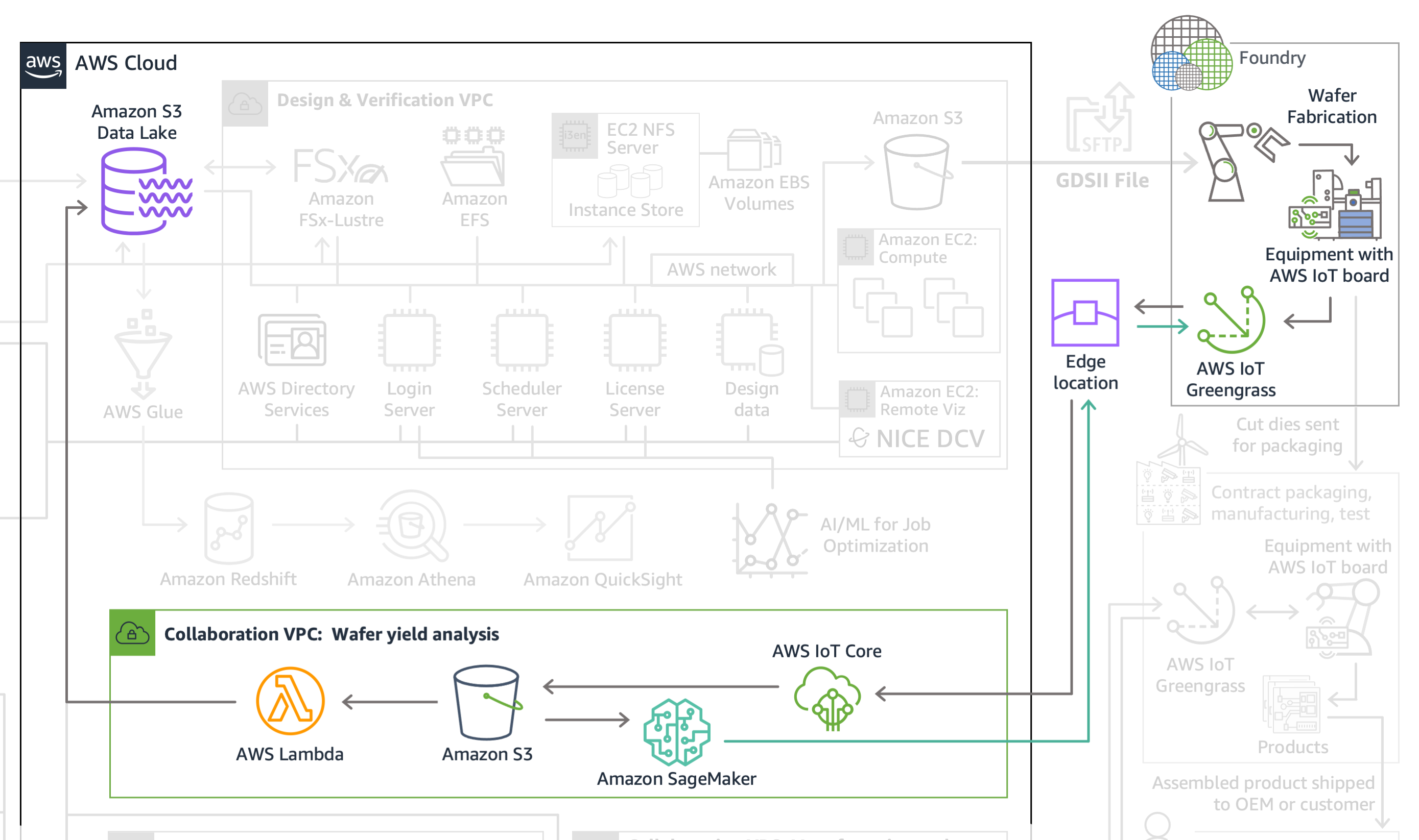
Collaboration with foundry - wafer yield analysis
As shown in the preceding figure, collaboration with your foundry starts with data
collection from an AWS IoT board that is installed in the on-premises foundry equipment.
The IoT board sends data to AWS IoT Greengrass
Similar to the collaborative efforts with the IP providers and EDA tool vendors, the resulting wafer data is sent to the same data lake used for the entire semiconductor design workflow.
Collaboration with packaging and contract manufacturers
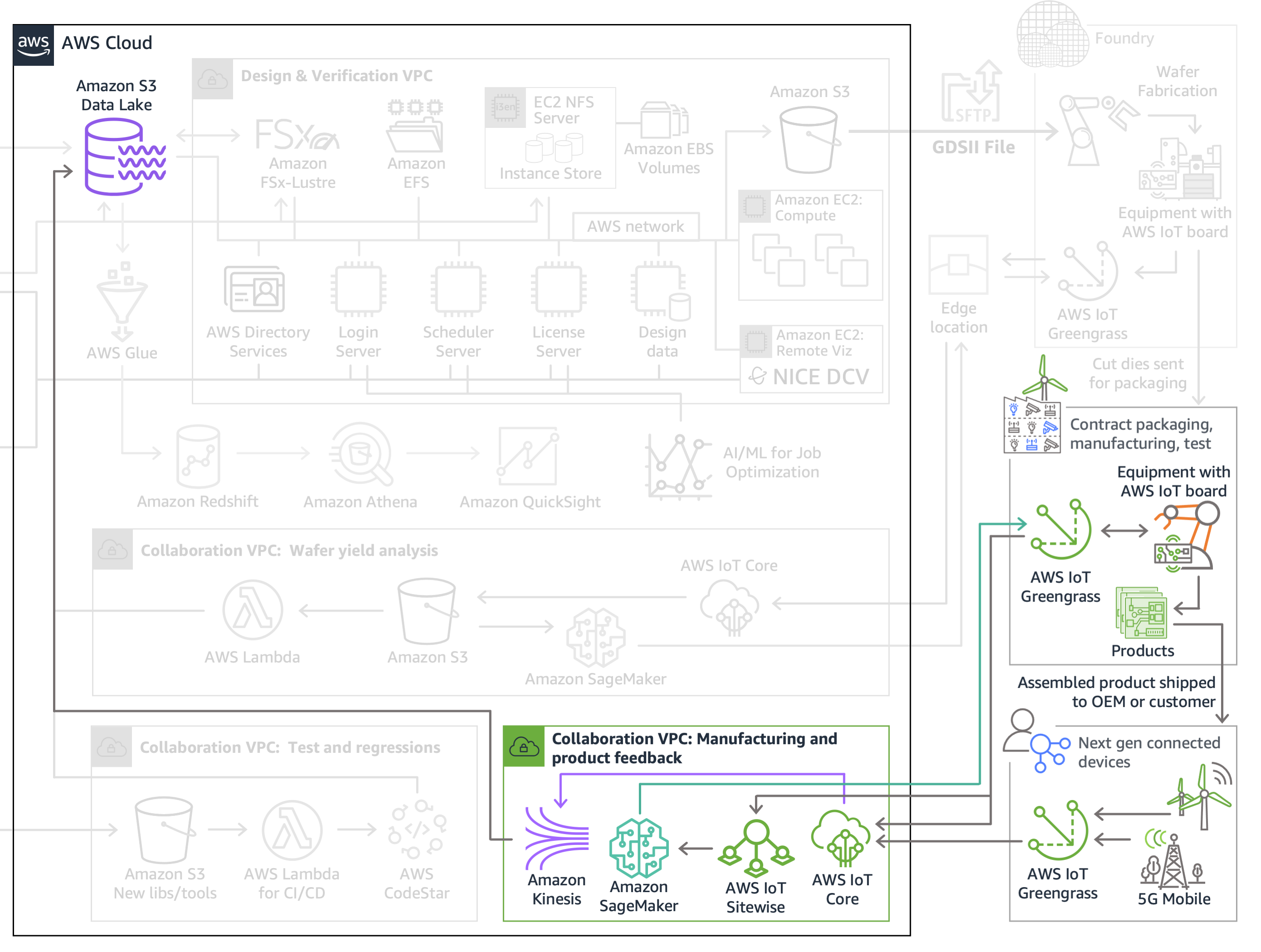
Similar to the way collaboration is enabled with the foundry, you can also enable collaboration with your packaging and contract manufacturers, as well as the devices in the field. The following figure shows the workflow for collaboration with packaging and contract manufacturers.
Collaboration with packaging and contract manufacturers
In the preceding figure, data is sent to both AWS IoT Core and AWS IoT SiteWise using an
AWS IoT board that is installed in the on-premises manufacturing equipment. AWS IoT SiteWise
