Fabrication, packaging, and final product
Once the GDSII file is sent to the foundry, this initiates a process resulting in the delivery of the IC or device to the OEM or end user.
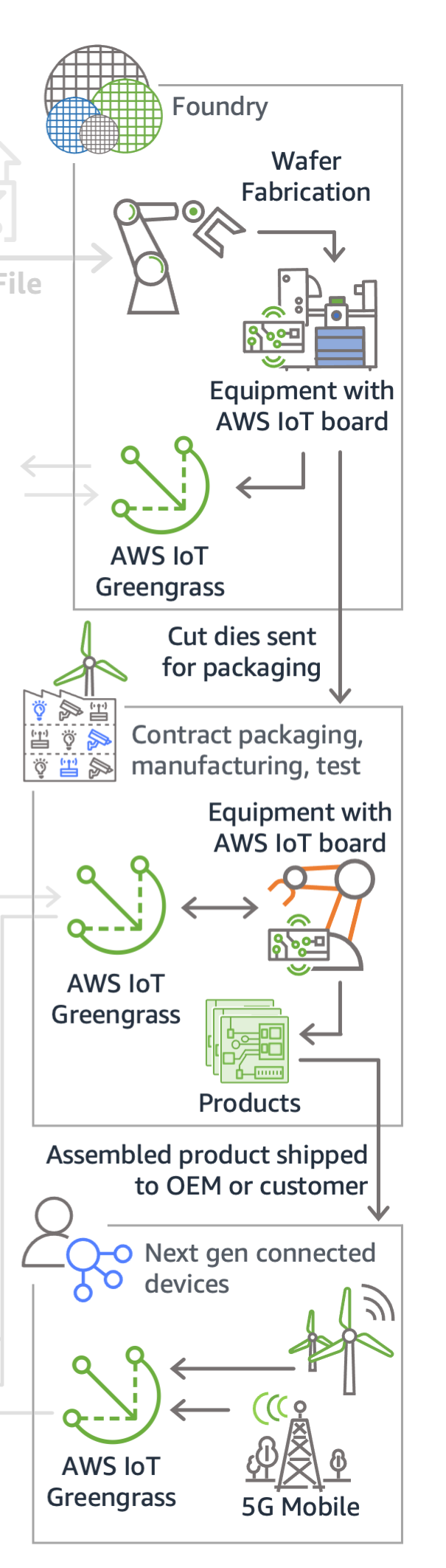
The following figure shows the process of fabricating the wafers, sending the cut dies for packaging, and sending the assembled product to the OEM or customer. Normally, the chip designer has little or no visibility for these processes. By introducing collaboration across the entire industry, time-to-market (TTM) can be reduced while increasing return on investment (ROI). The product of industry wide collaboration is comprehensive data collection of the entire workflow, from customer specification to products in the field. The data collected can then be analyzed using an analytics pipeline, entirely built on AWS. This pipeline results in insights and actions that can dramatically influence the way your teams design semiconductors.
Fabrication, packaging, and final product
