Launch and configure the entire semiconductor design workflow
With the combination of infrastructure already in place and the guidance from the
previous section, you can now launch and configure the entire workflow, to include scaling out
to 10,000s of cores. We recommend using the previously mentioned AWS Solutions Implementation
Scale-Out Computing on AWS
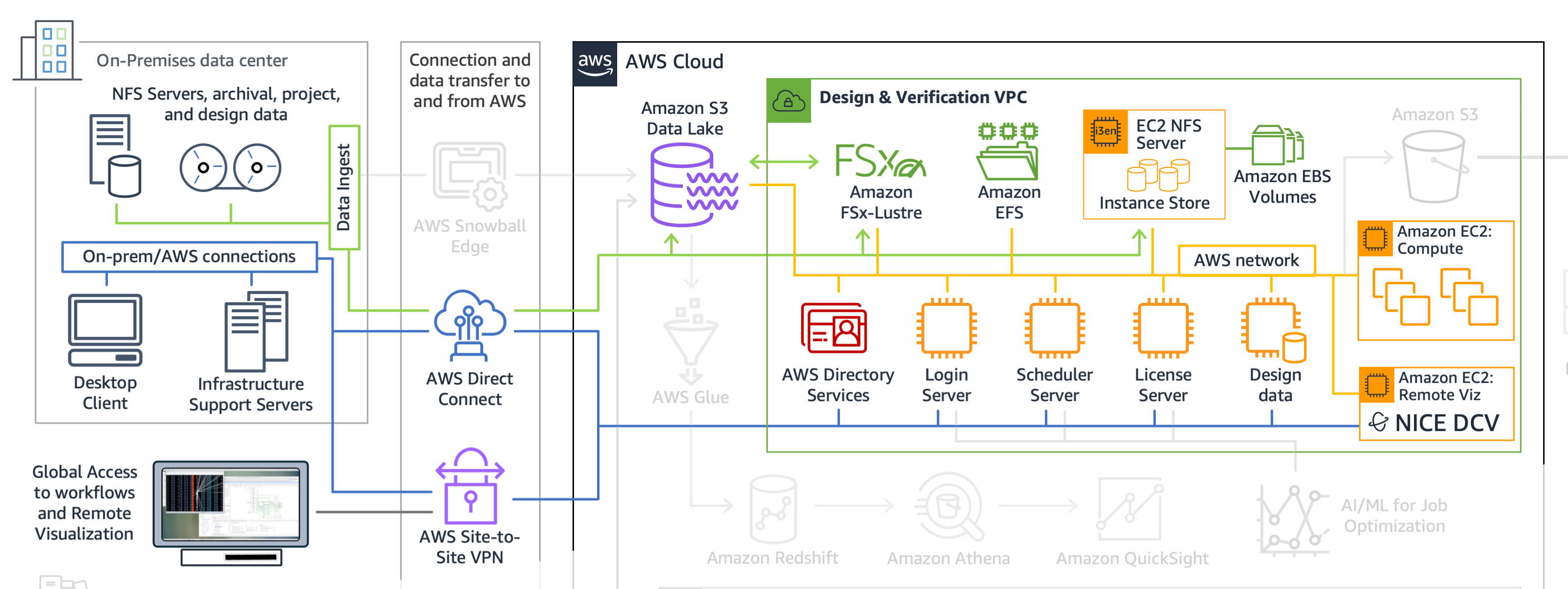
The following figure shows all of the necessary resources to run your entire
semiconductor design workflow on AWS. The previous section provided the details and guidance
for determining what compute, storage, file systems, and networking options are required.
Using Scale-Out Computing on AWS
Launch and configure the entire semiconductor design workflow
Building on the previously launched architecture used for your POC, the environment is now extended to handle additional storage options and scaling out compute resources to 10,000s of cores.
