This whitepaper is for historical reference only. Some content might be outdated and some links might not be available.
Semiconductor and Electronics on AWS - High Level
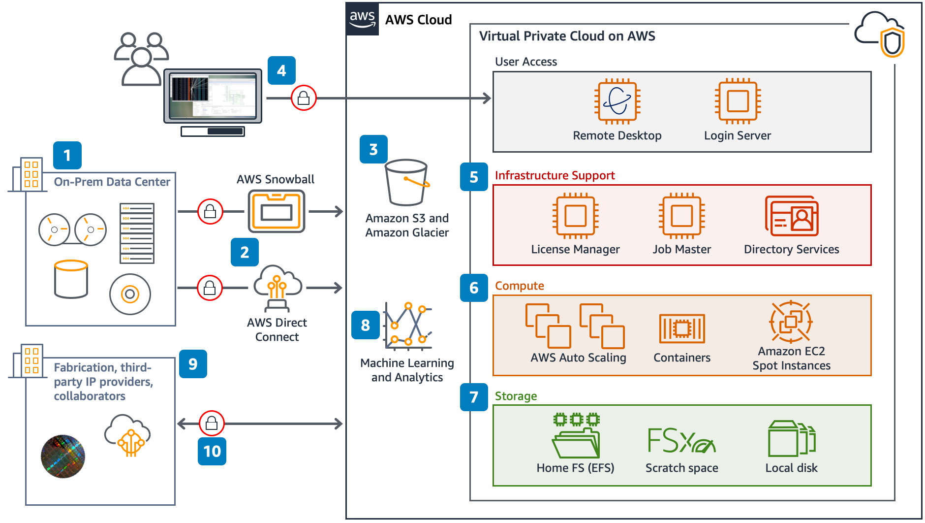
The following architecture diagram shows migration of workflows to AWS and a high-level architecture for running semiconductor design workflows. In this architecture diagram, the infrastructure that is running on AWS is similar to the previous on-premises environment diagram. This simple architecture helps you understand the high-level approach without the need for knowing the details about each of the services that is used.
Semiconductor and Electronics Design on AWS - High Level
Table 1 – Semiconductor and Electronics Design on AWS - High Level desciptions
| Callout | Description |
|---|---|
| 1 | Determine what data is needed for proof of concept or test. |
| 2 | Transfer data into AWS via AWS Snowball Edge, AWS Direct Connect, or using several other AWS services. |
| 3 | Transferred data is stored in Amazon S3 buckets. You can access data stored in Amazon S3 from an Amazon EC2 instance or nearly any AWS service. |
| 4 | Users access their environment through a remote desktop session or command line (ssh). |
| 5 | All of the infrastructure needed for semiconductor design workflows is available on AWS. |
| 6 | AWS compute is flexible and robust, more than capable of running semiconductor design workflows |
| 7 | Store tools and job data on Amazon EFS, Amazon FSx for Lustre, and local disk. Optionally, move long-term data storage to Amazon S3. |
| 8 | Once your data is in AWS, you can leverage other services, such as data lakes, AI/ML, and analytics. |
| 9 | Isolating environments leads to enhanced security and limits third parties to only the data they need. |
| 10 | Encryption is everywhere and can be enabled with your encryption keys. |
